With the rapid advancement of semiconductor chip and MEMS sensor industries, high‑end smart manufacturing sets rigorous standards for production‑site cleanliness and waste‑gas emission compliance.
Core production workflows including semiconductor etching, wafer cleaning, chip packaging & testing, and sensor R&D continuously generate mixed acid‑alkali waste gas and VOCs. Improper abatement not only impairs precision equipment performance and product yield, but also brings substantial environmental compliance risks. For semiconductor manufacturers, a stable, high‑efficiency and custom‑engineered waste‑gas treatment system is therefore a critical foundation for safe, clean and environmentally‑responsible operations.
For years, CADAIR has specialized in developing and deploying waste‑gas abatement solutions tailored to high‑end semiconductor manufacturing. Backed by proprietary technologies, proven solutions and full‑cycle support services, CADAIR delivers reliable environmental protection for a broad portfolio of semiconductor and sensor manufacturers.
Recently, a batch of CADAIR VOCs and waste‑gas treatment projects across Beijing, Shanghai and Zhejiang have passed final acceptance and entered official operation. These projects serve multiple high‑end semiconductor segments, covering scientific instrumentation & equipment, image‑sensor packaging‑and‑testing, and MEMS sensor manufacturing.
Recently Accepted & Commissioned Projects
These three completed projects are built for complex on‑site operating conditions with strict emission requirements, delivering targeted resolutions for waste‑gas and exhaust‑ventilation pain points in diverse semiconductor manufacturing scenarios. Key project profiles are shown below.
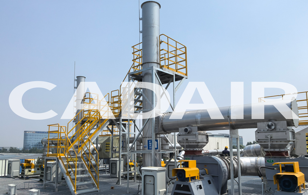
1. Waste‑Gas Treatment Project|Beijing Beiguang Communication High‑End Instrument & Equipment R&D Base
Custom‑built for R&D and manufacturing of high‑end semiconductor instruments and equipment, this project addresses mixed VOCs and acid‑alkali waste gas generated from on‑site production activities.
- Air‑handling capacity: 30,000 m³/h
- Core treatment processes: Scrubber pre‑treatment | Deep purification via activated‑carbon adsorption
- Project value: Effectively removes mixed factory‑site waste gas; consistently satisfies cleanliness specifications for R&D‑oriented production and statutory emission standards; secures a safe working environment for precision instrument research and manufacturing.
2. Exhaust‑Ventilation Retrofit Project|OmniVision Semiconductor (Shanghai) Image‑Sensor Back‑End Packaging & Test Facility
Focused on back‑end packaging‑and‑test procedures for image sensors, this initiative upgrades the legacy exhaust‑ventilation system to resolve insufficient throughput and poor adaptability to actual production conditions.
- Air‑handling capacity: 6,200 m³/h
- Core processes: Existing exhaust‑ventilation system optimization & retrofit | Pipeline layout upgrade | Exhaust efficiency improvement
- Project value: Eliminates poor air circulation and waste‑gas accumulation inside packaging‑and‑test workshops; optimizes on‑site manufacturing environment; fully adapts to high‑precision sensor packaging‑and‑test operating requirements.
3. Waste‑Gas Treatment Project|Quzhou Lanxin Semiconductor High‑Performance MEMS Sensor Manufacturing Plant (Zhejiang)
A large‑scale integrated waste‑gas abatement system designed for mass‑production MEMS‑sensor fabs, targeting high‑concentration VOCs and acid‑alkali waste gas from volume‑production processes.
- Air‑handling capacity: 90,000 m³/h
- Core treatment processes: Scrubber‑based acid‑alkali neutralization pre‑treatment | Advanced purification with activated‑carbon adsorption
- Project value: Stable performance under large air‑volume conditions with qualified waste‑gas removal efficiency; fulfills dual core objectives: regulatory environmental compliance and clean manufacturing for high‑output semiconductor factories.
Three Core Advantages of CADAIR for Semiconductor Waste‑Gas Treatment
The successful acceptance and commissioning of these projects further demonstrate CADAIR’s strong technical strength within high‑end semiconductor waste‑gas abatement. Driven by differentiated strengths in technology, service and real‑world project references, CADAIR has become a trusted supplier for many leading semiconductor enterprises.
✦ Full‑Lifecycle Closed‑Loop Services for Efficient & Reliable Project Delivery
Moving beyond simple equipment supply‑only business models, CADAIR provides end‑to‑end closed‑loop services: site investigation, custom solution engineering, equipment fabrication, installation & commissioning, acceptance filing, operator training and ongoing after‑sales maintenance.
Dedicated project engineers offer one‑on‑one support throughout the whole implementation cycle. Facing complex semiconductor working conditions, equipment‑parameter matching challenges and tricky on‑site commissioning scenarios, our team dynamically optimizes technical proposals to accelerate project roll‑out and ensure smooth acceptance and stable long‑term operation for every delivered system.
✦ Extensive Real‑World Project Portfolio, Market‑Validated Practical Capabilities
With long‑term focus on semiconductor‑grade VOCs and acid‑alkali waste‑gas treatment, CADAIR has accumulated rich hands‑on experience in high‑end manufacturing projects.
At present, more than 1,300 sets of our treatment equipment are running reliably at client sites across thousands of enterprises. Our business scope covers semiconductor chips, MEMS sensors, advanced new materials, fine chemicals, automotive manufacturing and other high‑value industries. Mass completed field projects verify CADAIR equipment’s strengths of stable operation, convenient maintenance and rapid technical response, building solid safeguards for customers’ safe production and green compliance targets.
✦ Authoritative Technical Recognition, Leading Compliant Treatment with Industry‑Standard‑Setting Strength
CADAIR develops proprietary core waste‑gas‑abatement technologies that have obtained national‑level official recognition. Our zeolite‑rotor concentration technology is listed in the National Catalogue of Major Encouraged Environmental‑Protection Technologies and Equipment.
Meanwhile, CADAIR takes an active role in leading and participating in the drafting of multiple national environmental‑protection industry standards. Leveraging benchmark‑level technical competence for semiconductor waste‑gas projects, we maintain industry‑leading performance on compliance guarantee, solution professionalism and equipment reliability, precisely matching the stringent environmental and manufacturing requirements of the semiconductor sector.